- 您现在的位置:买卖IC网 > Sheet目录336 > LC4064ZC-EV (Lattice Semiconductor Corporation)BOARD EVAL FOR ISPMACH 4064ZC
�� �
�
�Lattice� Semiconductor�
�ispMACH� 4000V/B/C/Z� Family� Data� Sheet�
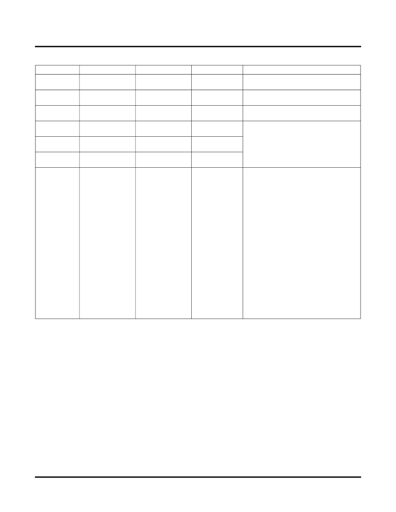
�ispMACH� 4000V/B/C/Z� Power� Supply� and� NC� Connections� 1� (Cont.)�
�Signal�
�VCC�
�132-ball� csBGA� 7�
�P1,� A14,� B7,� N8�
�144-pin� TQFP� 4�
�36,� 57,� 108,� 129�
�176-pin� TQFP� 4�
�42,� 69,� 88,� 130,�
�256-ball� ftBGA/fpBGA� 2,� 3,� 7,� 9�
�B2,� B15,� G8,� G9,� K8,� K9,� R2,� R15�
�157,� 176�
�VCCO0�
�G3,� P5,� C1� 8� ,� M2� 8� ,�
�3,� 19,� 34,� 47,� 136�
�4,� 22,� 40,� 56,� 166�
�D6,� F4,� H7,� J7,� L4,� N6�
�VCCO� (Bank� 0)� C5�
�VCCO1�
�M10,� M14� 8� ,� H12,�
�64,� 75,� 91,� 106,� 119� 78,� 92,� 110,� 128,�
�D11,� F13,� H10,� J10,� L13,� N11�
�VCCO� (Bank� 1)� A10,� C13� 8�
�144�
�GND�
�B1,� P2,� N14,� A13�
�1,� 37,� 73,� 109�
�2,� 46� 5� ,� 65,� 90,� 134,� A1,� A16,� C6,� C11,� F3,� F14,� G7,� G10,� H8,�
�153�
�H9,� J8,� J9,� K7,� K10,� L3,� L14,� P6,� P11,� T1,�
�10,� 18� ,� 27,� 46,� 127,� 13,� 31,� 55,� 155,�
�GND� (Bank� 0)�
�E2,� K2,� N4,� B4�
�137�
�6�
�167�
�T16�
�GND� (Bank� 1)�
�N11,� K13,� E13,� B11� 55,� 65,� 82,� 90� 6� ,� 99,�
�118�
�67,� 79,� 101,� 119,�
�143�
�NC�
�4064Z:� C1,� C3,� E1,�
�4128V� :� 17,� 20,� 38,�
�1,� 43,� 44,� 45,� 89,�
�4256V/B/C,� 128� I/O:� A4,� A5,� A6,� A11,� A12,�
�E3,� H2,� J3,� K1,� M2,�
�M4,� N5,� P7,� P8,� M8,�
�P10,� P11,� P14,� M12,�
�K14,� K12,� G13,�
�G14,� E14,� C13,� B13,�
�B10,� C10,� A7,� B5,�
�A5,� A4,� A1�
�4128Z:� P8,� A7�
�45,� 72,� 89,� 92,� 110,� 131,� 132,� 133�
�117,� 144�
�4256V� :� 18,� 90�
�A13,� A15,� B5,� B6,� B11,� B12,� B14,� C7,� D1,�
�D4,� D5,� D10,� D12,� D16,� E1,� E2,� E4,� E5,� E7,�
�E10,� E13,� E14,� E15,� E16,� F1,� F2,� F15,� F16,�
�G1,� G4,� G5,� G6,� G12,� G13,� G14,� J11,� K3,�
�K4,� K15,� L1,� L2,� L12,� L15,� L16,� M1,� M2,� M3,�
�M4,� M5,� M12,� M13,� M15,� M16,� N1,� N2,� N7,�
�N10,� N12,� N14,� P5,� P12,� R4,� R5,� R6,� R11,�
�R12,� R16,� T2,� T4,� T5,� T6,� T11,� T12,� T13,�
�T15�
�4256V/B/C,� 160� I/O:� A5,� A12,� A15,� B5,� B6,�
�B11,� B12,� B14,� D4,� D5,� D12,� E1,� E4,� E5,�
�E13,� E15,� E16,� F1,� F2,� F15,� G1,� G5,� G12,�
�G14,� L1,� L2,� L12,� L15,� L16,� M1,� M2,� M3,�
�M12,� M16,� N1,� N12,� N14,� P5,� R4,� R5,� R6,�
�R11,� R12,� R16,� T4,� T5,� T12,� T15�
�4384V/B/C:� B5,� B12,� D5,� D12,� E1,� E15,�
�E16,� F2,� L12,� M1,� M2,� M16,� N12,� R5,� R12,�
�T4�
�4512V/B/C:� None�
�1.� All� grounds� must� be� electrically� connected� at� the� board� level.� However,� for� the� purposes� of� I/O� current� loading,� grounds� are� associated� with�
�the� bank� shown.�
�2.� Internal� GNDs� and� I/O� GNDs� (Bank� 0/1)� are� connected� inside� package.�
�3.� V� CCO� balls� connect� to� two� power� planes� within� the� package,� one� for� V� CCO0� and� one� for� V� CCO1� .�
�4.� Pin� orientation� follows� the� conventional� order� from� pin� 1� marking� of� the� top� side� view� and� counter-clockwise.�
�5.� ispMACH� 4384V/B/C� pin� 46� is� tied� to� GND� (Bank� 0).�
�6.� ispMACH� 4128V� only.�
�7.� Pin� orientation� A1� starts� from� the� upper� left� corner� of� the� top� side� view� with� alphabetical� order� ascending� vertically� and� numerical� order�
�ascending� horizontally.�
�8.� ispMACH� 4128Z� and� 4256Z� only.� NC� for� ispMACH� 4064Z.�
�9.� Use� 256� ftBGA� package� for� all� new� designs.� Refer� to� PCN#14A-07� for� 256� fpBGA� package� discontinuance.�
�44�
�发布紧急采购,3分钟左右您将得到回复。
相关PDF资料
LCMXO2280C-C-EVN
BOARD CONTROL EVAL MACHXO
LDB100-024SW
LED POWER SUPPLY 24V 0-4A 100W
LDB150-048SW
LED POWER SUPPLY 24V-48V 3.125A
LDB200-048SW
LED POWER SUPPLY 24V-48V 4.2A
LDB75-048SW
LED POWER SUPPLY 24V-48V 1.56A
LDS8141-002-T2
IC LED DRIVER WHIT BCKLGT 16WQFN
LDS8160-002-T2
IC LED DVR WHT/RGB BCKLGT 16WQFN
LDS8620-002-T2
IC LED DRIVER FLASH 16WQFN
相关代理商/技术参数
LC4064ZE4MN100C
制造商:LATTICE 制造商全称:Lattice Semiconductor 功能描述:1.8V In-System Programmable Ultra Low Power PLDs
LC4064ZE4MN100CES
制造商:LATTICE 制造商全称:Lattice Semiconductor 功能描述:1.8V In-System Programmable Ultra Low Power PLDs
LC4064ZE4MN100I
制造商:LATTICE 制造商全称:Lattice Semiconductor 功能描述:1.8V In-System Programmable Ultra Low Power PLDs
LC4064ZE4MN100IES
制造商:LATTICE 制造商全称:Lattice Semiconductor 功能描述:1.8V In-System Programmable Ultra Low Power PLDs
LC4064ZE4MN144C
制造商:LATTICE 制造商全称:Lattice Semiconductor 功能描述:1.8V In-System Programmable Ultra Low Power PLDs
LC4064ZE-4MN144C
功能描述:CPLD - 复杂可编程逻辑器件 64MC 64 I/O Ultra Low Power 1.8V
RoHS:否 制造商:Lattice 系列: 存储类型:EEPROM 大电池数量:128 最大工作频率:333 MHz 延迟时间:2.7 ns 可编程输入/输出端数量:64 工作电源电压:3.3 V 最大工作温度:+ 90 C 最小工作温度:0 C 封装 / 箱体:TQFP-100
LC4064ZE4MN144CES
制造商:LATTICE 制造商全称:Lattice Semiconductor 功能描述:1.8V In-System Programmable Ultra Low Power PLDs
LC4064ZE4MN144I
制造商:LATTICE 制造商全称:Lattice Semiconductor 功能描述:1.8V In-System Programmable Ultra Low Power PLDs